Welcome to the official website of Henan Boyan New Materials Co., Ltd!


News Center
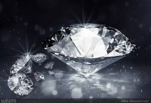
Development status of diamond semiconductor materials
Release Time:
2025-07-14 11:19
Diamond crystal preparation
Diamond is used in the semiconductor industry, and large-sized single crystal materials are required. The preparation method of diamond crystals is also constantly developing, and various CVD (Chemical Vapor Deposition) technologies are mainly used. In the 21st century, the emergence of repeated growth methods, three-dimensional growth methods and mosaic methods has promoted the development of large-scale diamond preparation, and once again set off a wave of research and preparation of diamonds.
The advancement of diamond material preparation technology is the driving force behind the performance improvement of diamond electronic devices. Internationally, British Element Six, Japan Institute of Industrial Technology (AIST), Japan Institute of Materials Research (NIMS), American Geophysical Laboratory Carnegie Institute, Argonne National Laboratory, etc. have been committed to diamond material technology. Upgrade.
British Element Six is a leader in the synthesis of high quality (electronic grade) CVD diamond single crystals. In 2004, a large size electronic scale single crystal of 5 mm × 5 mm was grown. The total impurity content can be controlled at 5 ppb (ppb is 1 billion). One of the points), with a dislocation density of 103-104/cm2, is the main supplier of high-quality single crystals required for the development of global diamond transistors, diamond quantum communication technology and diamond high-energy particle detectors. In terms of polycrystalline, commercial production of electronic grade 4-inch polycrystalline diamond has been realized.
In 2012, the Carnegie Institute of the United States announced that it has made significant progress in the manufacture of chrome-grade colorless CVD diamonds, producing a colorless single crystal diamond that weighed 2.3 carats after processing and grew at a rate of 50 μm/h. Moreover, it has been realized that square diamond grows simultaneously on six faces, making it possible to grow large single crystal diamond.
Japan's AIST used MPCVD in 2010 to produce single crystal diamonds up to 12 mm and 25 mm mosaic wafers. In 2013, AIST continued to expand its crystal size and obtained 38.1 mm (1.5 inch) diamond chips. In 2014, 50.8 mm (2 inches) single crystal diamond was successfully obtained by homoepitaxial technology and mosaic growth technology, but its impurity and dislocation density. high.
In 2017, the University of Augsburg in Germany realized large-size single crystal diamond materials with a diameter of 92 mm and 155 carats by heteroepitaxial technology, providing a new technical approach for the development of large-size single crystal diamonds, but due to heteroepitaxial growth. Lead to higher dislocation density.
Doping technique
The biggest problem in achieving the commercialization of diamond semiconductor devices is the difficulty in doping, especially for n-type doping. P-type doping is relatively easy. At present, diamond-doped p-type materials are basically mature and practical. However, this method requires high temperature (1450 ° C) heating, which leads to multiple crystal packing, and the fabricated semiconductor device does not perform as well as a single crystal. If the method of implanting boron atoms in the crystal production process to achieve doping of the diamond single crystal, not only high injection power but also the performance of the diamond crystal is required.
In 2016, the United States made a breakthrough in diamond doping technology, and developed a new low-temperature doping process, which can achieve the doping of boron atoms in diamond single crystals at a lower temperature, which is simple, inexpensive, and easy to operate. At the heart of the new process is the addition of "silicon" by attaching a layer of boron-doped silicon to the diamond single crystal and then heating it to 800 °C to transfer the boron atoms from the silicon to the diamond. By attaching silicon to a special position on the surface of the diamond crystal, it is possible to produce diamond with specific properties, thereby achieving selective doping, achieving higher control in device fabrication, and further development of the diamond semiconductor device. . Since the method realizes p-type doping, the n-type doping problem is still not solved, and the next step is to overcome the problem of n-type doping to realize devices such as transistors.
development,the,of,diamond,in,and,to,crystal,single,is
Contact Us
Email:boyan@boyan9.com
Contact:+86-13510564526
Address: No.7, Road 7, Economic Zone, Yichuan County, Luoyang City, Henan Province
Scan to view the mobile website
Copyright © 2019 Henan Boyan New Materials Co., Ltd.